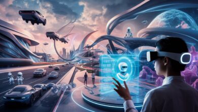
From the first bulky computers dotting the landscape of the tech world to the miniaturized, multifaceted devices we carry in our pockets, the evolution of electronics has been nothing short of spectacular. Amidst this ongoing revolution, there exists a groundbreaking innovation that is poised to redefine the benchmarks for performance and efficiency in next-generation electronics — Nanosetfld technology.
But what exactly is Nanosetfld technology, and how does it promise to revolutionize the electronics industry? In this comprehensive guide, we’ll explore the ins and outs of Nanosetfld technology and its applications, paint a picture of what the future might hold, and provide a glimpse into the dynamic world that’s unfolding with its adoption.
Introduction to Nanosetfld Technology
Nanosetfld technology represents a leap from the micro- to the nanoscale, allowing for the fabrication of devices that function at extraordinarily small dimensions. At its core, Nanosetfld technology involves the manipulation and control of materials at the level of individual atoms or molecules, harnessing the unique properties that emerge at such scales.
In the context of electronics, the application of this technology has the potential to create devices that are not only vastly more powerful but also significantly smaller and more energy-efficient. The promise of Nanosetfld technology is to enable electronics that can perform complex tasks with minimal resources, opening the door to a new era of innovation.
Applications in Next-Gen Electronics
Nanosetfld technology’s reach extends across a wide spectrum of electronic devices that permeate the fabric of our daily lives. In next-generation smartphones, the use of nanosetfld materials can result in screens that are more responsive, batteries with a higher energy density, and processors that operate at blazing speeds without overheating.
Wearables, too, stand to benefit from Nanosetfld technology, with the potential for devices that are not only more discreet and comfortable but also better at monitoring our health with sensors that are more sensitive and accurate.
IoT devices can become even more ubiquitous and blend more seamlessly with our environment, thanks to Nanosetfld technology enabling tiny yet incredibly powerful computing and communication components.
Advantages of Nanosetfld Technology
The integration of Nanosetfld technology in electronics carries with it a plethora of benefits. By working at the nanoscale, engineers can take advantage of materials that exhibit extraordinary conductivity, exponentially increasing the efficiency of energy transfer and ensuring that even the most complex tasks draw only minimal power.
Furthermore, the miniaturization of electronic components allows for the creation of products that are more portable and less obtrusive, all while still packing a substantial technological punch. The enhanced performance capabilities also future-proof devices, ensuring they can handle the demands of tomorrow’s applications without being rendered obsolete.

Challenges and Limitations
While the promise of Nanosetfld technology is undeniable, its integration into real-world devices is not without its challenges. One significant hurdle is the complexity of manufacturing devices at such precise scales, which requires cutting-edge facilities and specialized equipment.
Cost is another factor that could hinder widespread adoption. The investment required to set up and operate nanoscale manufacturing facilities is substantial, and these costs could potentially trickle down to consumers, making Nanosetfld-powered electronics a premium option.
Scalability is also an issue that needs to be addressed. The technology may work on a small scale, but mass production of nanoscale components that meet quality standards and maintain consistency across numerous identical units is a significant undertaking.
Future Trends and Innovations
The future of Nanosetfld technology in electronics promises to be an exciting one, with ongoing research focusing on pushing the boundaries of what is possible. Innovators are looking to harness the potential of quantum computing at the nanoscale, which could lead to electronic devices that process information in fundamentally different ways, with profound implications for fields such as artificial intelligence and cryptography.
Materials science is also a hotbed of activity, with researchers endeavoring to discover and synthesize nanosetfld materials that possess novel properties, opening up new avenues for performance enhancements in electronic devices.
Case Studies
The potential of Nanosetfld technology is not just theoretical; several notable case studies exist that demonstrate its viability and practical application in electronic devices.
In the smartphone sector, certain models already make use of nanosetfld coatings to make their devices water-resistant, showcasing one of the technology’s more immediately accessible benefits.
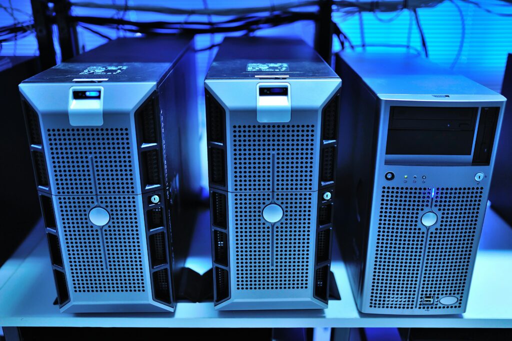
In the semiconductor industry, manufacturers are steadily incorporating nanosetfld materials into their chip designs, resulting in processors and memory units that are both faster and more energy-efficient, and in the case of memory, more capacious.
Conclusion
Nanosetfld technology is the tiny revolution that could have an enormous impact on the world of electronics. With the potential to enhance everything from the smallest sensor to the most powerful supercomputers, its applications are far-reaching and diverse.
While challenges such as manufacturing complexities and costs remain, the advantages promised by Nanosetfld technology are too significant to ignore. With continued research and investment, we are inching closer to a world where small is not just beautiful but also incredibly powerful.
For tech enthusiasts, electronics manufacturers, and innovators alike, keeping a close eye on the trajectory of Nanosetfld technology is crucial as it paves the way for the next frontier in electronic innovation.